










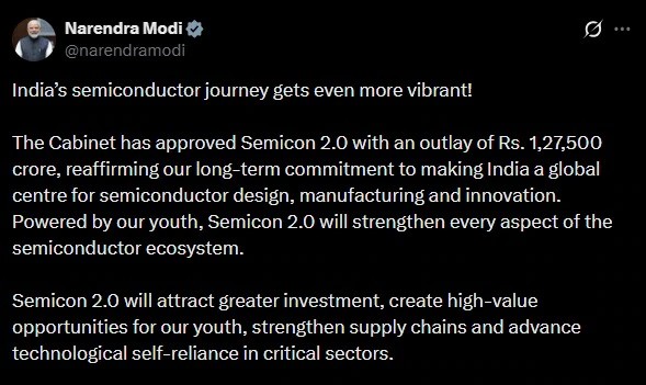
New Delhi: The Union Cabinet has approved Semicon 2.0, the second phase of the India Semiconductor Mission (ISM), with a total outlay of Rs 1,27,500 crore, marking India’s biggest investment yet in building a self-reliant semiconductor ecosystem. The ambitious programme aims to expand the country’s capabilities across the entire semiconductor value chain, from chip design and fabrication to research, packaging, equipment manufacturing and talent development.
The approval follows the progress made under Semicon 1.0, which was launched in December 2021 with an allocation of Rs 76,000 crore. While the first phase focused primarily on establishing semiconductor manufacturing facilities, Semicon 2.0 broadens the scope to develop a comprehensive chip ecosystem that can support India’s long-term technological and economic ambitions.
Prime Minister Narendra Modi described the initiative as a major step towards strengthening India’s technological self-reliance and attracting global investments into the country’s semiconductor industry.
Building on the foundation of Semicon 1.0
The first phase of the India Semiconductor Mission laid the groundwork for India’s semiconductor manufacturing ambitions.
According to government data, 12 semiconductor manufacturing projects with cumulative investments exceeding Rs 1.64 lakh crore have been approved under Semicon 1.0.
These include:
- One silicon fabrication plant (fab)
- One silicon carbide fabrication facility
- One integrated gallium nitride (GaN) Micro LED display fab
- Nine semiconductor packaging units
These projects are expected to serve industries such as consumer electronics, automotive, industrial electronics, telecommunications, aerospace and power electronics.
Among the notable projects are Tata Electronics’ semiconductor fabrication facility in Dholera, Gujarat, and Micron Technology’s assembly and testing plant, both of which represent significant milestones in India’s semiconductor journey.
Several approved facilities, including those operated by Micron, Kaynes and CG Semi, have already commenced commercial production.
Growing semiconductor design ecosystem
Apart from manufacturing, Semicon 1.0 also focused on strengthening India’s chip design capabilities.
The government has approved 24 semiconductor design projects submitted by startups and MSMEs, while more than 105 startups and MSMEs have received access to industry-standard Electronic Design Automation (EDA) tools.
These companies are developing semiconductor solutions for applications including:
- Artificial Intelligence (AI)
- Internet of Things (IoT)
- Drones
- Satellite communications
- Smart meters
- Telecom equipment
- Surveillance systems
- LED drivers
India has also announced indigenous processors such as Dhruv64 and Vikram32, demonstrating growing domestic design capabilities.
Meanwhile, around 315 universities have adopted professional chip-design software for training purposes, helping nearly 68,000 students acquire semiconductor design skills.
Six pillars of Semicon 2.0
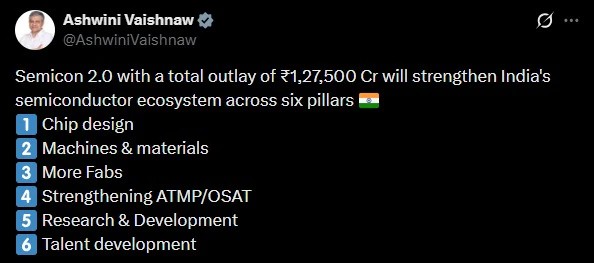
Electronics and IT Minister Ashwini Vaishnaw said Semicon 2.0 has been designed around six strategic pillars to create a complete semiconductor ecosystem.
The six focus areas include:
- Semiconductor design
- Machines and materials
- More fabrication plants
- Assembly, Testing, Marking and Packaging (ATMP) and Outsourced Semiconductor Assembly and Test (OSAT)
- Research and Development (R&D)
- Talent development
Unlike the first phase, which concentrated largely on manufacturing incentives, Semicon 2.0 aims to strengthen every stage of semiconductor production.
Greater emphasis on manufacturing ecosystem
A key addition under Semicon 2.0 is support for companies manufacturing semiconductor equipment, chemicals, specialty gases and materials essential for chip fabrication.
The programme also seeks additional investments in:
- Silicon fabs
- Compound semiconductor fabs
- Display fabrication units
- Discrete semiconductor manufacturing
By encouraging domestic production of critical materials and equipment, the government aims to reduce India’s dependence on imported semiconductor supply chains.
Industry experts believe localisation of these supporting industries is essential for long-term competitiveness.
Focus on advanced research
Semicon 2.0 also expands support for semiconductor research and development.
The programme aims to encourage work on advanced semiconductor process technologies beyond the 28nm to 110nm manufacturing nodes currently targeted under many domestic projects.
The government plans to collaborate with Indian and international research institutions to accelerate innovation in advanced chip manufacturing technologies.
For comparison, many of today’s flagship smartphone processors are manufactured using 3nm and 4nm process technologies.
Developing skilled workforce
Talent development remains another major component of Semicon 2.0.
The government plans to expand semiconductor education at the university level while introducing more industry-led training programmes covering:
- Cleanroom operations
- Fab construction
- Semiconductor manufacturing
- Equipment maintenance
- Packaging technologies
These initiatives are expected to create a larger pool of highly skilled engineers capable of supporting India’s growing semiconductor industry.
The government has indicated that detailed implementation guidelines for Semicon 2.0 are likely to be notified within the coming weeks.
Industry sees long-term opportunity
Industry experts believe Semicon 2.0 represents a significant policy shift towards building a sustainable semiconductor ecosystem.
Analysts note that semiconductor fabrication requires long investment cycles, often taking nearly a decade before achieving full-scale commercial maturity.
Experts also believe expanding beyond manufacturing into design, research, equipment and materials will make India’s semiconductor industry less dependent on imports and better integrated into global supply chains.
The government has highlighted growing interest from companies based in the United States, Europe, Japan, Singapore, Germany and the Netherlands, with firms including Applied Materials, AMD, Microchip Technology, Lam Research and KLA already announcing investments or partnerships in India.
Conclusion
With an allocation of Rs 1.27 lakh crore, Semicon 2.0 represents India’s most ambitious semiconductor initiative to date. Building on the foundation established under Semicon 1.0, the programme seeks to develop a complete semiconductor ecosystem encompassing design, manufacturing, research, packaging and talent development. While meaningful results will take several years to materialise, the initiative is widely viewed as a crucial step towards reducing import dependence, strengthening supply chain resilience and positioning India as a major player in the global semiconductor industry.