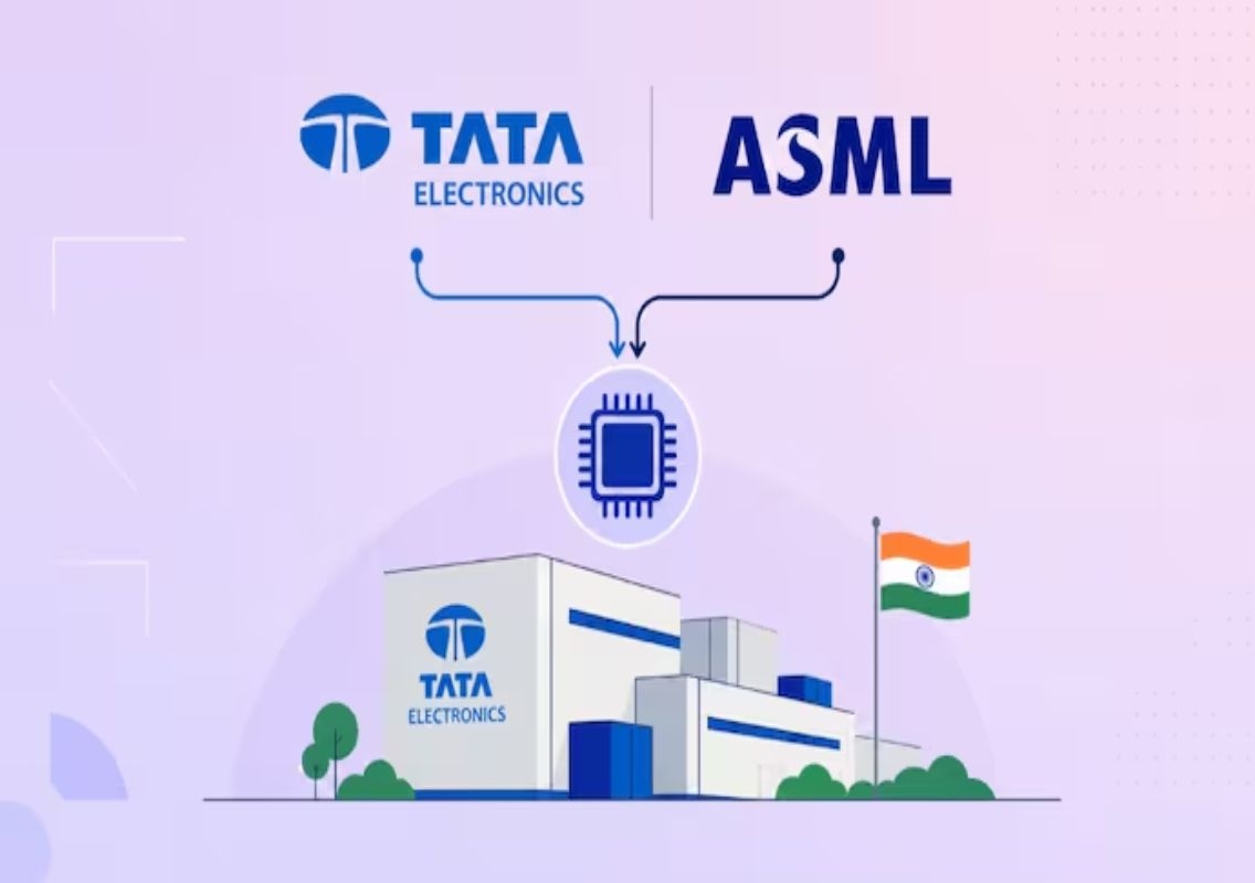
New Delhi: Tata Electronics has signed a significant agreement with Dutch technology leader ASML, marking a crucial step in India’s efforts to build a domestic semiconductor manufacturing ecosystem. While the deal focuses on enabling 300mm wafer production in India, its broader implications could be far more transformative for the country’s silicon chip ambitions.
The agreement, announced on Saturday, may appear technical on the surface. However, industry experts believe it signals India’s growing credibility in the global semiconductor supply chain and could pave the way for future access to more advanced chip-making technologies.
Why ASML matters globally
ASML, short for Advanced Semiconductor Materials Lithography, is one of the most critical companies in the global technology ecosystem. Unlike consumer-facing giants, it operates behind the scenes but plays an indispensable role in semiconductor manufacturing.
The company is the only manufacturer of extreme ultraviolet (EUV) lithography machines, which are essential for producing cutting-edge chips used in smartphones, artificial intelligence systems and advanced computing. These machines enable the creation of extremely small transistors, going down to 2 nanometres, making them vital for high-performance chips.
Despite its importance, ASML remains relatively unknown outside specialised tech circles. Yet, nearly every modern electronic device depends, directly or indirectly, on its technology.
Understanding the Tata-ASML agreement
The partnership centres around Tata Electronics’ semiconductor fabrication plant being set up in Dholera, Gujarat. This facility is expected to be India’s first commercial semiconductor fab and could begin production by the end of the year.
There are two critical aspects in semiconductor manufacturing: the fabrication process and the wafer size.
For fabrication technology, Tata is collaborating with Powerchip Semiconductor Manufacturing Corporation. The process nodes are expected to range between 110 nanometres and 28 nanometres. While 28nm is not cutting-edge by global standards, it is sufficiently advanced for a wide range of applications such as automotive electronics, consumer devices and industrial systems.
The partnership with ASML focuses on wafer technology, specifically enabling 300mm wafers. Larger wafers allow more chips to be produced per batch, improving efficiency and reducing costs. Currently, 300mm is considered the global industry standard.
No EUV yet, but a strategic start
It is important to note that the agreement does not include ASML’s advanced EUV machines. These machines are highly restricted and are currently available only in a few countries, including the United States, Japan, South Korea and Taiwan.
Each EUV system costs around $400 million (approximately Rs 3,855 crore), and exports are tightly controlled due to their strategic importance. As a result, India will initially rely on deep ultraviolet (DUV) lithography systems, which are less advanced but still critical for large-scale semiconductor manufacturing.
However, experts suggest that the presence of ASML in India could act as a catalyst for future advancements. Even without EUV technology, collaboration can help build technical expertise, workforce skills and operational discipline.
Building India’s semiconductor ecosystem
The Tata-ASML partnership is not just about equipment or production. It represents a broader effort to develop a complete semiconductor ecosystem in India.
Industry analysts point out that chip manufacturing requires more than fabrication plants. It involves a network of suppliers, including materials, chemicals, design firms and testing facilities.
The collaboration is expected to contribute to knowledge transfer, skill development and process standardisation — all of which are essential for long-term success in the semiconductor industry.
India has already taken steps in this direction, with initiatives such as indigenous chip development and new fabrication proposals in regions like Noida.
Strategic and geopolitical significance
The agreement also carries geopolitical importance. Semiconductor supply chains are increasingly seen as strategic assets, with countries seeking to reduce dependence on a few dominant players.
By partnering with ASML, Tata Electronics positions India as a credible destination for semiconductor investments. The deal sends a positive signal to global players that India is serious about becoming part of the semiconductor value chain.
The presence of leaders such as Narendra Modi and Rob Jetten during the agreement highlights its diplomatic and economic significance.
Conclusion
The Tata-ASML partnership marks an important milestone in India’s semiconductor journey. While it does not immediately bring cutting-edge chip manufacturing capabilities, it lays the groundwork for future growth.
By enabling 300mm wafer production and fostering collaboration with a global technology leader, the deal strengthens India’s position in the semiconductor ecosystem. Over time, such partnerships could help the country move up the value chain and reduce reliance on imports.
As India continues to invest in infrastructure, talent and policy support, the collaboration with ASML could prove to be a turning point in realising its silicon chip ambitions.